The following was the description of the goals associated with this challenge:
"For this retrochallenge. I want to completely redesign the PCB so it has the same dimensions as the original: 111 mm tall / 50 mm wide. While the display will remain the not period-accurate LED, all the components will be placed so that their centerline is in the same position as the originals. The board might end up being used with an enclosure, so components will be placed away from the edges such that a smaller version can be be quickly manufactured. Lastly, for aesthetic reasons, the board will have the same color scheme as the calculator and the traces will be discreetly run in the back, as much as possible."
The calculator at that time looked like this:
While it was an improvement over the Green V1 PCB, it was not quite the right dimension, the buttons were not placed with the correct spacing and there were some visible traces in the front. The circuit was also based on the KIM-1 and while it worked, I now realize that it was not the most efficient use of I/O pins for this particular combination of keys and digits.
The initial goals were somewhat easy, redesign the above circuit so it is size accurate and no traces in the front.
At the time, I already knew how to conceal vias by tenting them (placing soldermask and silkscreen over them. The following project log shows the technique:
https://hackaday.io/project/91895-sinclair-scientific-calculator-emulator/log/123664-12252017-finished-routing-the-board-and-submited-for-production
I had already learned how to do a keyboard label using negative silkscreen as shown in the project log:
https://hackaday.io/project/91895-sinclair-scientific-calculator-emulator/log/143883-01232018-slimmer-black-and-white-v2-board-sent-to-production
Another PCB design technique learned during this month was how to create custom PCB shapes. This can be as discreet as a rectangle with rounded corners or as exotic as an insect shape board:
https://hackaday.io/project/91895-sinclair-scientific-calculator-emulator/log/144392-how-to-design-a-custom-pcb-shape-for-fritzing-no-more-sharp-corners
By playing with an actual Sinclair Scientific calculator and pressing multiple keys, the connections between the keyboard the the display were deduced without disassembling the unit:
https://hackaday.io/project/91895-sinclair-scientific-calculator-emulator/log/144393-reverse-engineering-the-keyboard-and-display-circuit-on-a-real-sinclair-scientific
The following schematic was drawn using the information learned:
Using all these techniques, the following board was designed. The placement of the components matches the position of those of the real calculator. Most of the copper is in the bottom. Some unavoidable pieces are placed as long horizontal lines in the front. A couple of tracks that needed to go in the front were hidden under the 8 key.
View of the back of the board copper layer:
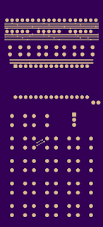
Copper in the front of the board:
An assembly guide was put together showing how to solder all the components;
https://hackaday.io/project/91895-sinclair-scientific-calculator-emulator/log/145323-assembly-instructions-for-pcb-v6
And here are pictures of the evolution of this project:
The latest version is placed next to the original
Overall, I am satisfied with the progress of this project. The latest version (V6) implements a calculator that is dimensionally and electrically correct.
All of the lessons learned are documented in the following page:
https://hackaday.io/project/91895-sinclair-scientific-calculator-emulator


